TSL1401CL
128 ?1 LINEAR SENSOR ARRAY WITH HOLD
TAOS136 JULY 2011
10
r
r
Copyright E 2011, TAOS Inc.
The LUMENOLOGY r Company
www.taosinc.com
APPLICATION INFORMATION: HARDWARE
PCB Pad Layout
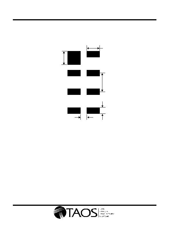
Suggested PCB pad layout guidelines for the CL package are shown in Figure 9.
0.8
0.8
1.3
1.4
2.5
Pin 1
NOTES: A. All linear dimensions are in millimeters.
B. This drawing is subject to change without notice.
Figure 9. Suggested CL Package PCB Layout
发布紧急采购,3分钟左右您将得到回复。
相关PDF资料
TSL1401CS-LF
IC OPTO SENSOR ARRAY CSP PCB MT
TSL1402R
IC LINEAR SENSOR ARRAY 256X1
TSL1406RS
IC LINEAR SENSOR ARRAY 768X1
TSL1410R
IC LINEAR SENSOR ARRAY 1280X1
TSL1412S
IC LINEAR SENSOR ARRAY 1536X1
TSL2014
IC LINEAR SENSOR ARRAY 896X1
TSL202R
IC LINEAR SENSOR ARRAY 128X1
TSL208R
IC LINEAR SENSOR ARRAY 512X1
相关代理商/技术参数
TSL1401CS
制造商:未知厂家 制造商全称:未知厂家 功能描述:128 1 LINEAR SENSOR ARRAY WITH HOLD
TSL1401CS-LF
功能描述:光频率和光电压 Linear Sensor Array 400dpi 128pix RoHS:否 制造商:ams 峰值波长:1000 nm 工作电源电压:5 V 最大工作温度:+ 85 C 最小工作温度:- 25 C 安装风格: 封装 / 箱体:
TSL1401R
功能描述:光频率和光电压 Linear Sensor Array 400dpi 128pix
RoHS:否 制造商:ams 峰值波长:1000 nm 工作电源电压:5 V 最大工作温度:+ 85 C 最小工作温度:- 25 C 安装风格: 封装 / 箱体:
TSL1401R-LF
功能描述:光频率和光电压 Linear Sensor Array 400dpi 128pix RoHS:否 制造商:ams 峰值波长:1000 nm 工作电源电压:5 V 最大工作温度:+ 85 C 最小工作温度:- 25 C 安装风格: 封装 / 箱体:
TSL1401USBEVM
功能描述:光学传感器开发工具 TSL1401 Eval Module with USB Interface RoHS:否 制造商:ams 工具用于评估: 接口类型: 最大工作温度:
TSL1402R
功能描述:光学开关,专业型 Linear Sensor 400 DPI RoHS:否 制造商:ams 感应方式: 安装风格:Through Hole 封装:Tube
TSL1406
制造商:未知厂家 制造商全称:未知厂家 功能描述:768 X 1 LINEAR SENSOR ARRAY WITH HOLD
TSL1406R
功能描述:光学开关,专业型 400 DPI SENSOR (2) 384 PIXEL SECT. RoHS:否 制造商:ams 感应方式: 安装风格:Through Hole 封装:Tube